

TOF-PET Test Device
Building and commissioning of a TOF-PET test device featuring SiPM read-out
Motivation
The aim of this project is to build and commission a multichannel Time-of-Flight Positron Emission Tomography (TOF-PET) test device with Silicon Photomultiplier (Multi- Pixel Photon Counter from HAMAMATSU ) read-out featuring a coincidence time resolution of about 300 ps FWHM. This corresponds to an improvement by a factor of two compared to commercially available devices which offer a time resolution of about 500 to 600 ps. A coincidence time resolution of 300 ps allows to locate the origin of the two back-to-back 511 keV Gamma rays with a precision of 4.5 cm FWHM. It has been shown that TOF information of this precision significantly improves the image quality. While for two channel systems coincidence time resolutions of 240 ps FWHM are achieved, it still has to be proven that similar results can be obtained with a multi-channel system with Silicon Photomultiplier read-out. Our TOF-PET device is meant to serve as a test bench for different multi-channel read-out electronics with high timing performance.
Description of the test device
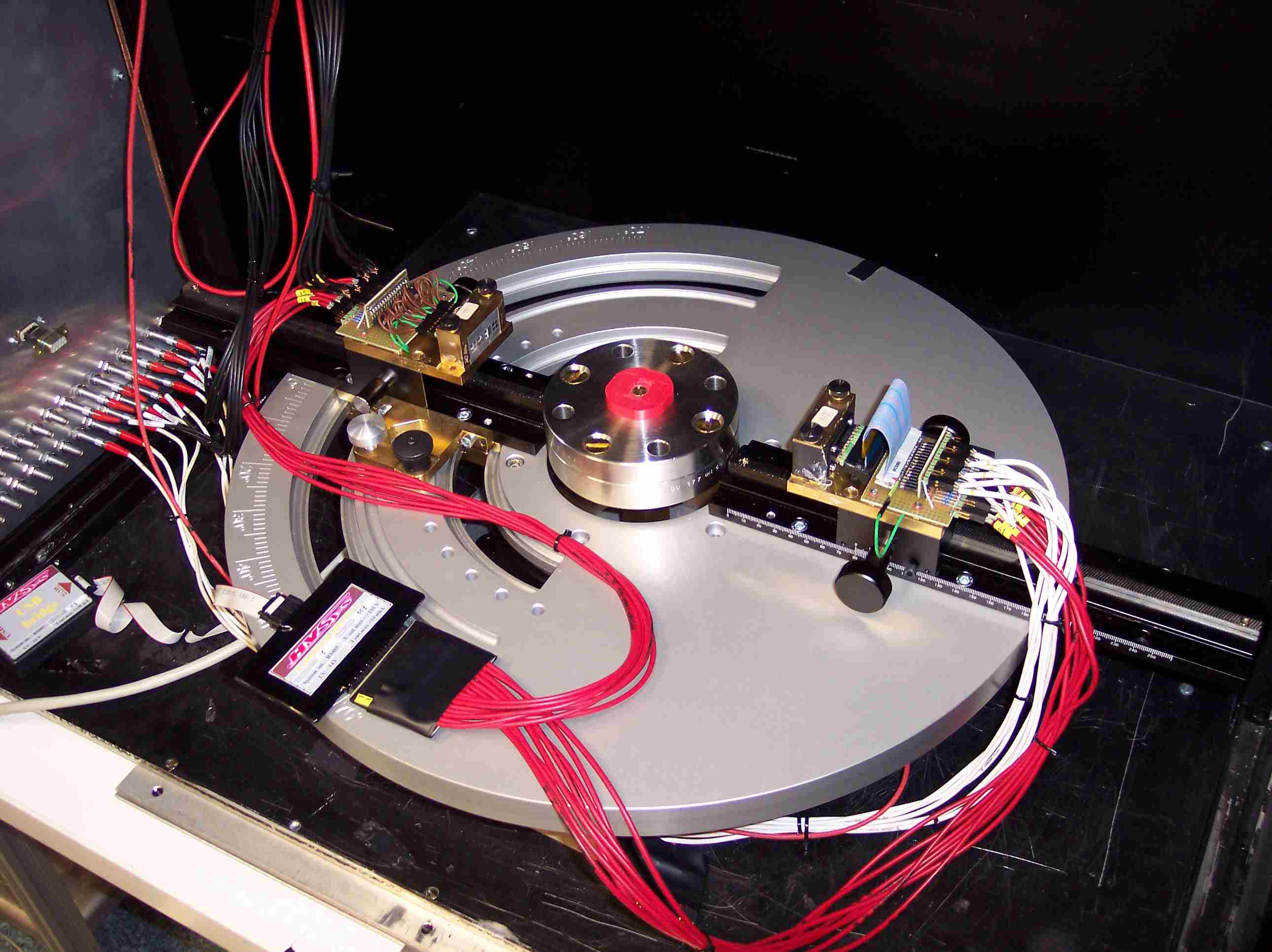
Figure 1: The TOFPET test device.
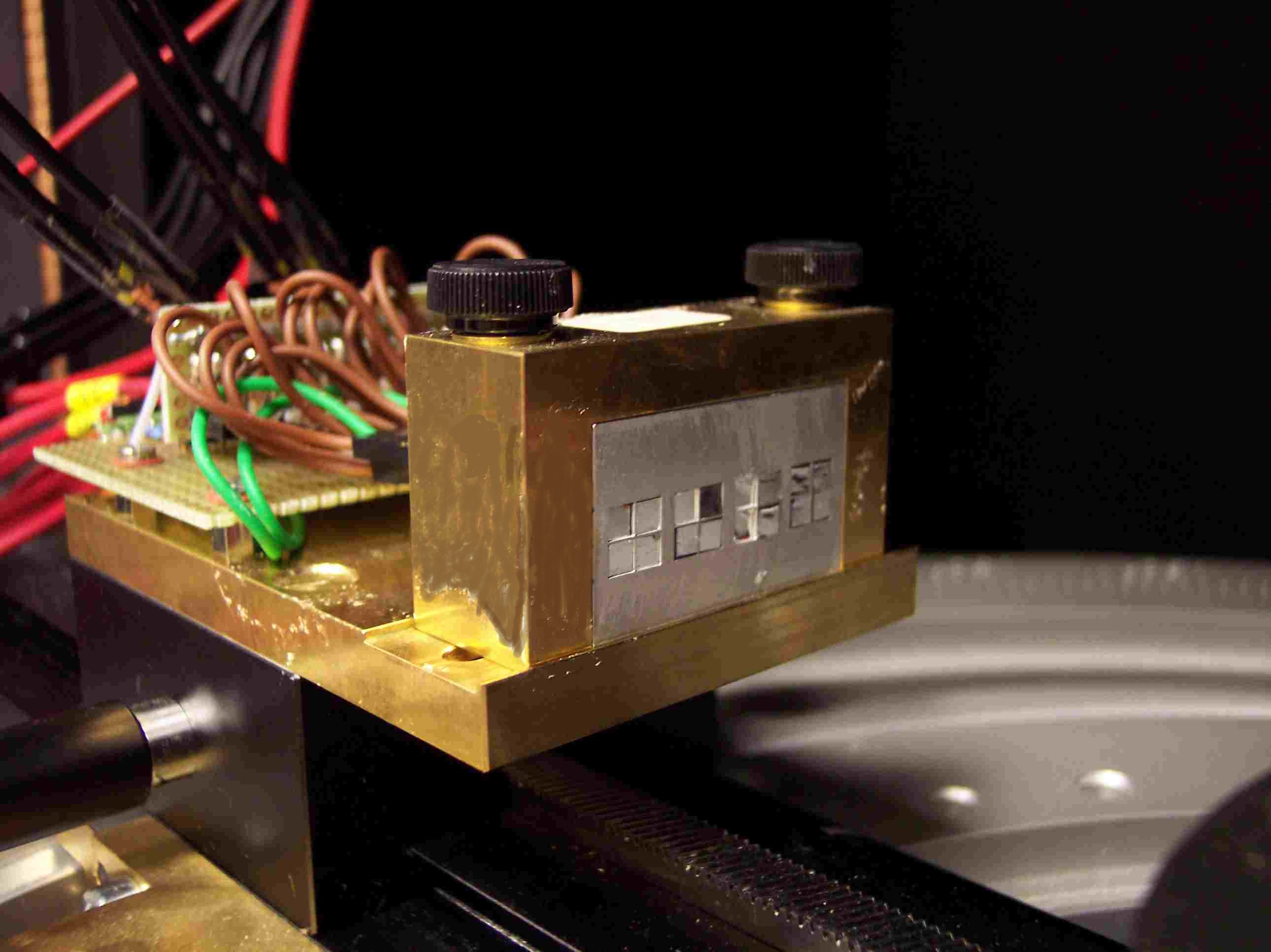
Figure 2: Full view of a single module.
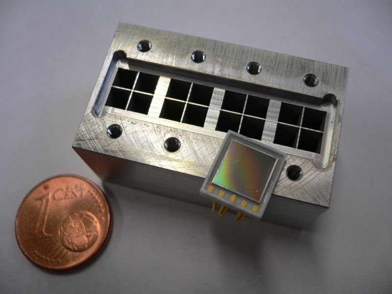
Figure 3: HAMAMATSU 2x2 MPPC array.
The cavities for the crystals are eroded by electrical discharge machining so that the individual crystals are separated by a 100 mum thick wall. The aluminium provides a very good reflectivity, hence, a good energy resolution is achieved. The bias voltage is provided by a multi-channel high voltage power supply ( HVSYS ) which allows to adjust the bias voltage for each MPPC device individually. The HV module is connected via a USB bridge to the USB port of a standard personal computer. A 16-channel 10-bit 100 MHz Flash ADC board with signal processing core ( ADCM-16 ) is used for the data acquisition. It is integrated on a CCB-PCI carrier board and utilizes one PCI slot of a computer. The device is capable to sustain high acquisitions rates up to a few hundred kHz. For the studies presented in this work only one crystal layer per module is read out, i.e. 8 channels for each module. We use this device only for a basic characterization of the system, as due to the 10 ns sampling the expected time resolution is not sufficient for our purpose. In the present study we use Multi-Pixel Photon Counter from HAMAMATSU to read out scintillating crystals (LFS). The MPPC shows a high sensitivity in the 450 nm spectral region. This matches the emission spectra of fast crystal scintillators which are peaked in the blue and ultra-violet spectral region, resulting in a high photon yield.
Contributing institutes
CERN, DESY, University of Heidelberg