

External Silicon Tracker
To validate the measured tracks in our Large Prototype TPC a silicon tracker will be installed as external reference. It needs to fit into the 3 cm space between the fieldcage wall of the Large Prototype and and inner wall of the 1 T magnet because a tracker outside of the magnet would suffer from the scattering of the test beam electrons in the magnet material and could not deliver the necessary resolution.
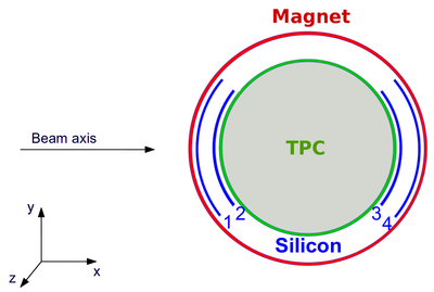
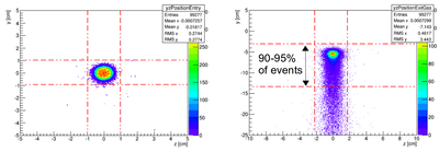
Simulation studies have been performed to determine the general characteristics of the system such as the number of silicon layers, the sensor spatial resolution and the coverage area of the system. Figure 1 shows a schematic layout of the system and Figure 2 the hit positions of beam particles in the front and back sensors indicating a minimum coverage area for the system.
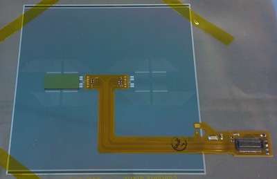
One of the main outcomes of the simulation studies is that the silicon sensors need to have a spatial resolution better than 10 μm. Exploring such possibilities, we are studying the use of silicon strip sensors of 25 μm pitch using KPiX chips for the readout as shown in Figure 3.
Currently, there is ongoing effort on the simulation of the system within the ILD framework (DD4HEP) as well as in the integration of the KPiX DAQ system to the DESY test beam. The mechanical support to fit the system in the existing infrastructure is under design.
Simulation studies have been performed to determine the general characteristics of the system such as the number of silicon layers, the sensor spatial resolution and the coverage area of the system. Figure 1 shows a schematic layout of the system and Figure 2 the hit positions of beam particles in the front and back sensors indicating a minimum coverage area for the system.
One of the main outcomes of the simulation studies is that the silicon sensors need to have a spatial resolution better than 10 μm. Exploring such possibilities, we are studying the use of silicon strip sensors of 25 μm pitch using KPiX chips for the readout as shown in Figure 3.
Currently, there is ongoing effort on the simulation of the system within the ILD framework (DD4HEP) as well as in the integration of the KPiX DAQ system to the DESY test beam. The mechanical support to fit the system in the existing infrastructure is under design.
Figure 1: Schematic layout of the silicon system and the current infrastructure.
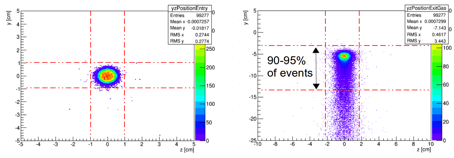
Figure 2: Simulated hit maps in the front (left) and back (right) silicon sensors. The broader distribution on the y axis for the back sensors (right) is a result of the magnetic field.
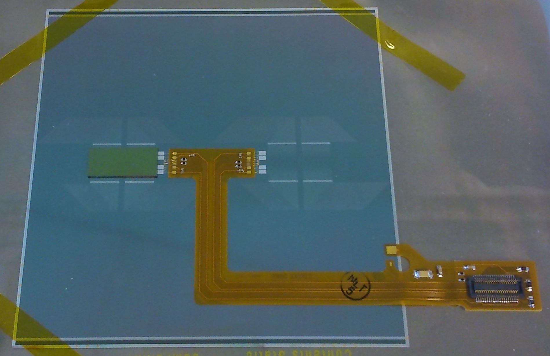
Figure 3: Silicon strip sensor with a bump bonded KPiX chip.