- Readout Of a Pad Plane with ElectRonics designed for pIxels
The idea
The aim of the project is to build and test a novel read out option for a time projection chamber (TPC).
The advantage of the high granularity of a pixelized read out, namely the Timepix chip, is combined
with the flexibility and high anode area coverage of a printed circuit board (PCB). This PCB needs to
be designed, built and tested.
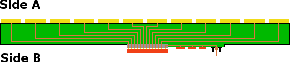
In figure 1 the scheme of the PCB is displayed: On side A sensitive pads receive electron avalanches a
GEM stack produced from drifting electron from the sensitive TPC volume. On side B a Timepix chip
is bump bonded to the PCB and reads in the signal through its input pixels. The output channels of the
chip are wire bond pads lying also on the „upper“ side of the chip, so they too are bump bonded to the
PCB side B. The chip output signal goes then into further read out and to a VHDCI connector. Inside
the board the foreseeably complex routing from the sensitive pads to the pixels needs to be done.
Figure 1: General struture of the ROPPERI PCB
The setup
The first prototype board will be tested with the UNIMOCS TPC at DESY. It consists of a 5cm drift
volume and a triple GEM stack with 10
x
10
cm
2 GEMs. The PCB will be part of the gas containment.
This way the VHDCI cable can go from the PCB directly to the SRS read out system which collects the
data and sends it via ethernet to a PC.
The UNIMOCS can be used with a radioactive source or with the DESY II test beam.
The challenges
In the long term the sensitive pads on the anode plane will have the size of a few hundred μm, the
Timepix chip has 256
x
256
=
65536 pixels with a pitch of 55
μm. The strip lines of typical FR-4 PCBs
have a pitch of >
100
μm and a via size of 350-500
μm. This limits the number of utilizable channels and
makes the routing quite complex.
Also, bump bonding with a pitch of 55
μm is nontrivial.
The Timepix chip was made for input capacitances of <
100
fF, with the PCB routing and strip lines of a
few cm they will be in the order of pF. This limits the signal-to-noise ratio.
The plan
The current plan foresees two prototype PCBs:
The first test board combines a limited number of channels (every 8
th pixel in x and y, 1024 channels)
with a range of different sensitive pad sizes and strip line lengths to check the signal/noise and to prove
the capability of the bump bonding.
The second test board will have a sensitive pad plane with specific sizes to identify electron clusters
from primary ionization in the active TPC volume. A larger number of channels is desired. The
necessary pad sizes will be determined via simulations.